|
■Structure of oxide-TFT-LCD
Orientation and feature of oxide TFT
Categorization of oxide TFTs
The top gate type
The conventional type
The self-align type
The bottom gate type
The etch-stopped type
The back-channel-etched type
The self-align type
The dual gate type
■Oxide-TFT array process
Forming process of gate electrode
Forming process of gate insulator film
Forming process of oxide semiconductor layer
Structure of oxide semiconductor layer
Deposition process of oxide semiconductor layer
Patterning process of oxide semiconductor layer
Direct printing of oxide semiconductor layer
Forming process of etch-stopped layer
Forming process of S/D
Forming process of passivation layer (+ planarization layer) and contact hole Anneal treatment
Forming process of pixel electrode
In case of use of inorganic transparent pixel electrode
In case of use of wettable material
Forming process of source/drain area
Forming process of top gate electrode
■CF (Color filter) forming process
Manufacturing process of CF for IPS mode/FFS mode TFT-LCD
Manufacturing process of CF for VA mode TFT-LCD
Manufacturing process of CF for TN/OCB mode TFT-LCD
Black matrix forming process
Manufacturing process of R, G, B color layer
Manufacturing process of overcoat layer
Deposition process of opposite electrode
Manufacturing process of post-spacer
Manufacturing process of rib (bump)
Photo-alignment process (for MVA mode TFT-LCD)
■LC cell process
Polyimid coating process
Alignment process
Seal layer forming process
Dispersion process of spacer-ball
Making panel thinner process
Scribe and break process
Filling process of LC material
ODF (One drop fill) process
■Module assemble process
Connect panel and driver-IC
■Liquid crystal material and display mechanism
■Structure of backlight module
Side light type
Light guide plate technology
Structure of direct type
LED backlight for TV (Direct type, side light type)
■Liquid crystal material and display mechanism
■3D technology
Method to use a specific glasses
LC shutter glasses method (Time sequential method)
Polarized glasses + patterned phase difference film (Space division method)
Specific glasses-free method
Parallax barrier method
Parallax barrier using dual emission OLED
Time sequential driving + parallax LC barrier method
Lenticular lens method
Time sequential twin-lens 3D-OCB method
Lenticular + time sequential scanning backlight method |
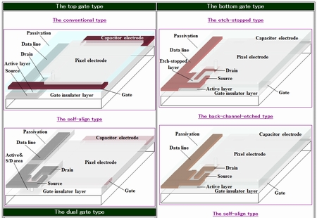
▲TFT structure
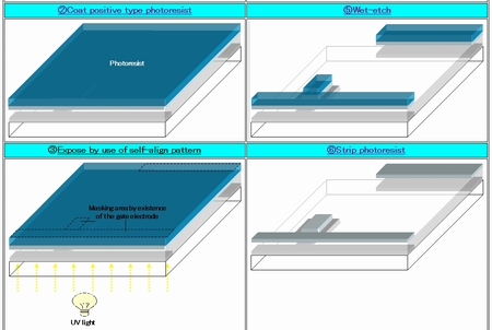
▲Self-alignment exposure process of the etch-stopped type TFT
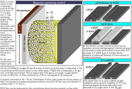
▲Structure of IGZO semiconductor layer
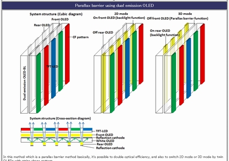
▲3D technology (Parallax barrier using dual emission OLED)
|