|
Categorization and manufacturing process of organic-TFT (General theory)
■Bottom gate/bottom contact structure
■Bottom gate/top contact structure
■Top gate/bottom contact structure
■Top gate/top contact structure
■Vertical type SIT (Static Induction Transistor)
Manufacturing process of organic-TFT (Particular theory)
■Forming process of gate electrode (Inorganic electrode)
■Forming process of gate electrode (Metal ink)
■Forming process of gate electrode (Conductive polymer)
■Forming process of gate insulator film
■Forming process of organic semiconductor layer
Evaporation process of small molecular organic semiconductor layer
Wet-coating process of wettable organic semiconductor
Alignment process of small molecular organic semiconductor
Surface modification process
Forming process of SAM film
■Forming process of inorganic S/D electrode (Vacuum deposition)
■Forming process of S/D electrode (Conductive polymer)
■Forming process of S/D electrode (Metal ink or paste)
■Forming process of S/D electrode (CNT)
Surface modification process
■Forming process of passivation layer
■Forming process of transparent pixel electrode
■Forming process of reflective pixel electrode
■Forming process of transparent pixel electrode (Conductive polymer, CNT, and Nano size Ag)
A word of caution in manufacturing of organic-TFT with flexible substrate
■Case of using flexible substrate with film shape
■Organic-TFT and device are manufactured on original substrate, and then transferred to plastic film
■Resin is coated on support substrate and cured, and then, organic-TFT and device are manufactured on resin film, finally, support substrate is released (the resin film is used as substrate)
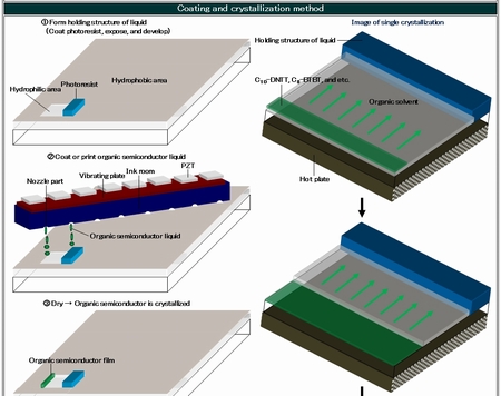
▲Process flow of single-like organic semiconductor
|
▲Process flow of bottom contact type organic-TFT
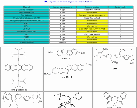
▲Organic semiconductor materials
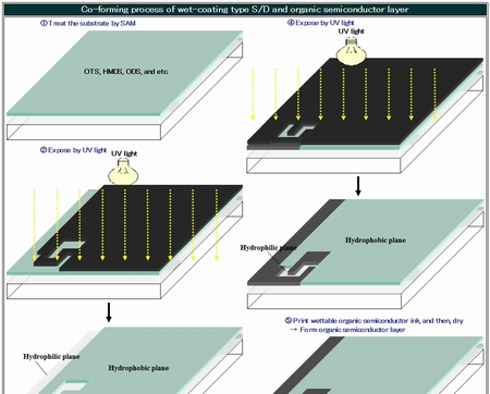
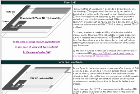
▲Co-forming process of S/D and organic semiconductor layer
|