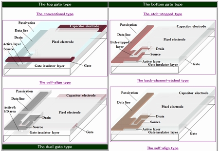
■Categorization and structure of oxide-TFT
Orientation and feature of oxide-TFT
Categorization of oxide-TFTs
The top gate type
The conventional type
The self-align type
The bottom gate type
The etch-stopped type
The back-channel-etched type
The self-align type
The dual gate type
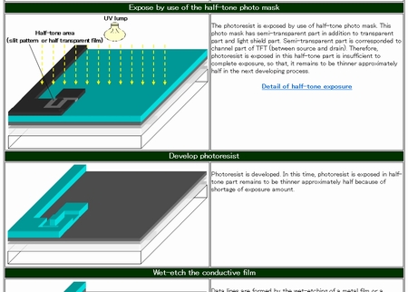
■Manufacturing process of the top gate type (general theory)
5 masks process
4 masks process
■Manufacturing process of the self-align type (general theory)
6 masks process
■Manufacturing process of the back-channel-etched type (general theory)
5 mask process
4 mask process
5 mask process (IGZO-TFT with n+ IGZO layer)
■Manufacturing process of the etch-stopped type (general theory)
6 masks process
■Manufacturing process of the back-channel-ethed type (The transparent TFT) (general theory)
4 masks process
■Manufacturing process of The dual gate type (general theory)
)
7 masks process
■Manufacturing process (particular theory)
Forming process of source/drain electrode
Forming process of oxide semiconductor layer (IGZO, AZTO, ZnO, HfIZO)
Forming process of using wettable oxide semiconductor material
Forming process of gate electrode
Forming process of gate insulator film
Forming process of source/drain area
Anneal treatment
Forming process of pixel electrode (inorganic transparent pixel electrode, reflection pixel electrode, wettable material
)
Forming process of passivation layer (+ the planarization layer) and the contact hole
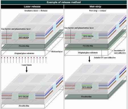
■A word of caution in manufacturing of oxide TFT with flexible substrate
Case of using flexible substrate with film shape
Oxide TFT and device are manufactured on original substrate, and then transferred to plastic film
Resin is coated on support substrate and cured, and then, oxide TFT and device are manufactured on resin film, finally, support substrate is released (The resin film is used as substrate)