|
Basic structure of OLED lighting device
üĪSmall molecular device and polymer device
üĪSingle unit device and multiple-unit device
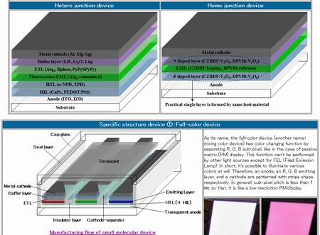
üĪHetero junction device and homo junction device
üĪSpecific structure device ć@üFFull-color device
üĪSpecific structure device ćAüFFine OLED array for the front light use
üĪHybrid device of OLED and organic film solar cell
Problem and solution example of OLED lighting device
üĪBoundary-less device
üĪAlloying device
Enhancement of light outcoupling efficiency
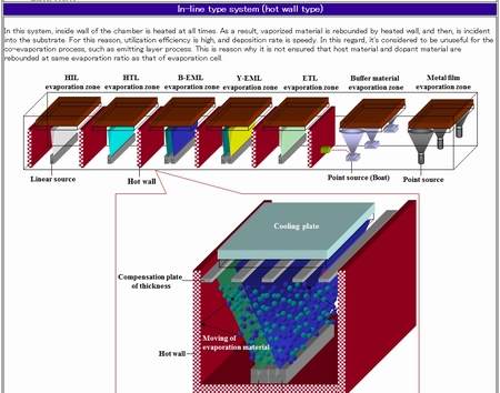
Process flow of OLED lighting device (general theory)ü@
üĪManufacturing process small molecular device (Single unit)
üĪManufacturing process small molecular device (Multiple-unit)
üĪManufacturing process of transparent device
üĪManufacturing process of small molecular device (Full-color device)
üĪManufacturing process polymer device (Single unit)
üĪManufacturing process polymer device (Multiple-unit)
üĪManufacturing process of polymer device (Full-color device)
ü@
Process flow of OLED lighting device (particular theory)ü@
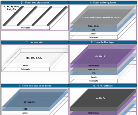
üĪForming process of bus electrode
üĪForming process of transparent anode
üĪForming process of hole injection layer
üĪForming process of hole transporting layer
üĪForming process of white emitting layer
üĪForming process of R, G, B emitting layer
üĪForming process of electron transporting layer/hole blocking layer
üĪForming process of alkali buffer layer/alkali doping layer
üĪForming process of CGL (Interlayer)
üĪForming process of transparent cathode
üĪForming process of metal cathode
üĪForming process of insulator layer
üĪForming process of cathode-separator
üĪSeal layer forming process
üĪEncapsulation process by cap glass
üĪEncapsulation process by flat glass
üĪEncapsulation process by the dam-fill method
üĪSolid encapsulation process
üĪThin film encapsulation process
üĪScribe and break process
|