Manufacturing process of organic film solar cell 2024


šExplain manufacturing process of organic film solar cell by illustration
šFull-cover from basic process to next generation process

šCover structure, substrate, material, manufacturing process, and encapsulation method
šIndicate molecule structure of organic material

šEasy to look at the file using any PC because of the format of browser, for example IE (Internet Explorer)
šPossible to access at will from Index Page to detail page
šDescribe these illustrations at 3D image
šNumber of total file are 31 (about 80 page in A4 form equivalent)
šIllustrations of device structure and process flow are approximately 180


MAIN CONTENT


¡Basic structure of organic film solar cell
Small molecular device and polymer device
p-n junction and bulk-hetero junction
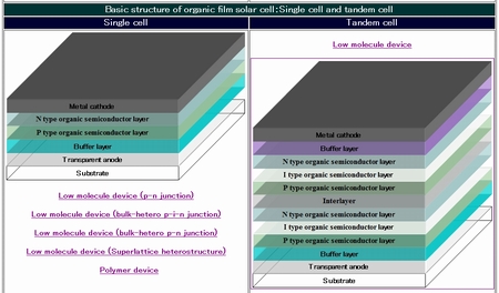
Single cell and tandem cell
Opaque device and transparent or semi-transparent device

¡Kind of device
Small molecular device (p-n junction)
Small molecular device (bulk-hetero p-i-n junction)
Small molecular device (bulk-hetero p-n junction)
Small molecular device (Superlattice heterostructure)
Polymer device (bulk-hetero junction)
Small molecular device (Tandem cell)
Polymer device (Tandem cell)
Hybrid device of small molecular unit and polymer unit (Tandem cell)
Transparent or semi-transparent device
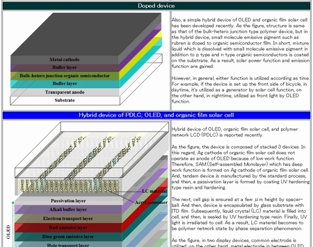
Hybrid device of OLED and organic film solar cell
Hybrid device of PDLC, OLED, and organic film solar cell

¡Process flow (general theory)
P-n junction type small molecular device (Single cell)
P-i-n junction type small molecular device (Single cell)
P-n bulk-hetero junction type small molecular device (Single cell)
Superlattice heterostructure small molecular device
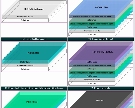
Polymer type device (Single cell)
P-i-n junction type small molecular device (Tandem cell)
Polymer type device (Tandem cell)
Hybrid type device (Tandem cell)
Polymer type device (Transparent cell)

¡Process flow (particular theory)
Forming process of transparent anode
Deposition process of buffer layer (Anode side)
Deposition process of oganic semiconductor with Nano-rod shape
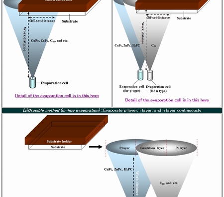
Forming process of small molecular organic semiconductor layer
Deposition process of buffer layer (Cathode side)
Forming process of metal cathode
Forming process of organic semiconductor layer (Wet-coat type device)
Forming process of interlayer
Forming process of transparent cathode

Seal layer forming process
Glass encapsulation process
@ Glass { glass
Solid encapsulation process
@ Single substrate device with glass
@ Single substrate device with plastic film
Thin film encapsulation process
@ Single substrate device with glass
Eencapsulation and insert process (Cylindrical device)
Scribe and break process


£Device structure


£Process flow of polymer device


£Structure sample of hybrid device


£Evaporation process of organic semiconductor layer

Full-original CD-ROM

CD-ROM for Windows • Macintosh
PriceF18,000 yen
Release dateFJanuary 4th 2024

While you order this CD-ROM, please input below points and send to info@e-express.co.jp.

CD-ROMForganic film solar cell manufacturing process
Campany's NameF
SectionF
NameF
AddressF
TELF
FAXF
e-mail addressF

Remark

If you are domestic customer, we will send the product and invoice. Please pay to ours account by bank remittance until specified date.

If you are overseas customer, we will send E-mail to you. Please pay to ours account by bank remittance. If we confirm bank transfer, we send the product immediately.


E Express Inc.
TELF+81-90-4203-4633(Kameya(President))
E-MailFinfo@e-express.co.jp

CD-ROM lists of English virsion

¡Manufacturing process of LTPS-TFT-LCD ¡Manufacturing process of oxide-TFT-LCD
¡Manufacturing process of a-Si TFT-LCD ¡Manufacturing process of oxide-TFT
¡Manufacturing process of OLED ¡Manufacturing process of OLED lighting device
¡Manufacturing process of organic film solar cell ¡Manufacturing process of E-paper display
¡Manufacturing process of FEL ¡Manufacturing process of organic-TFT
¡Manufacturing process of CNT-TFT ¡Manufacturing process of Perovskite solar cell

Go to the top page

@